COMPONENT Testing
- BGA/LGAs
- Package on Package (PoP)
- QFN/QFP/Die
Component testing is one of the most common applications for Akrometrix equipment. Akrometrix systems can test a large variety of component sizes and shapes through temperature. This testing is most commonly done on the attach side of components, with solder balls removed in the case of solder ball based SMT components.
In order to meet the testing throughput demands of many customers, component testing is very commonly done with high-volume thermal testing configurations. In these cases, the Part Tracking feature in Surface Measurement is often used. Part Tracking allows automatic location, rotation, and cropping of large sample quantities in a single reflow profile.
Warpage information on components is used in a number of ways, including:
- Failure Analysis: SMT failures can often be correlated with high levels of warpage found at the component level.
- Quality Assurance/Reliability: Shadow Moiré is being used, more and more often, to do lot to lot testing and perform outgoing QA for component manufacturers.
- Pass/Fail decisions: JEDEC and JEITA have established industry standards where warpage data can be compared with industry-accepted levels. These standards were written using data from Akrometrix systems.
- Shape Matching: Component shape can be oriented and matched with PCB local warpage information to perform gap analysis in the Akrometrix Interface Analysis software.
- Material and Design Choices: Different designs or materials in like form factors can be compared to find combinations with more favorable warpage profiles.
- FEA Model Validation: Component testing with Akrometrix equipment can be used in comparison with FEA simulation of component behavior over temperature.
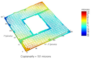
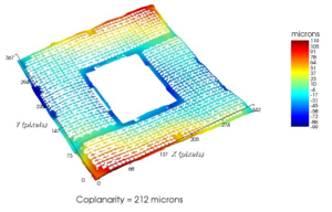
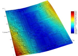
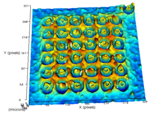
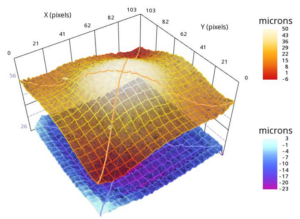
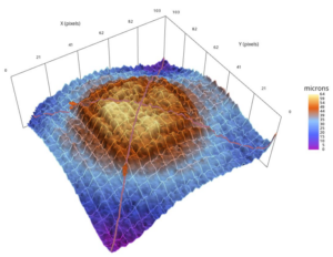
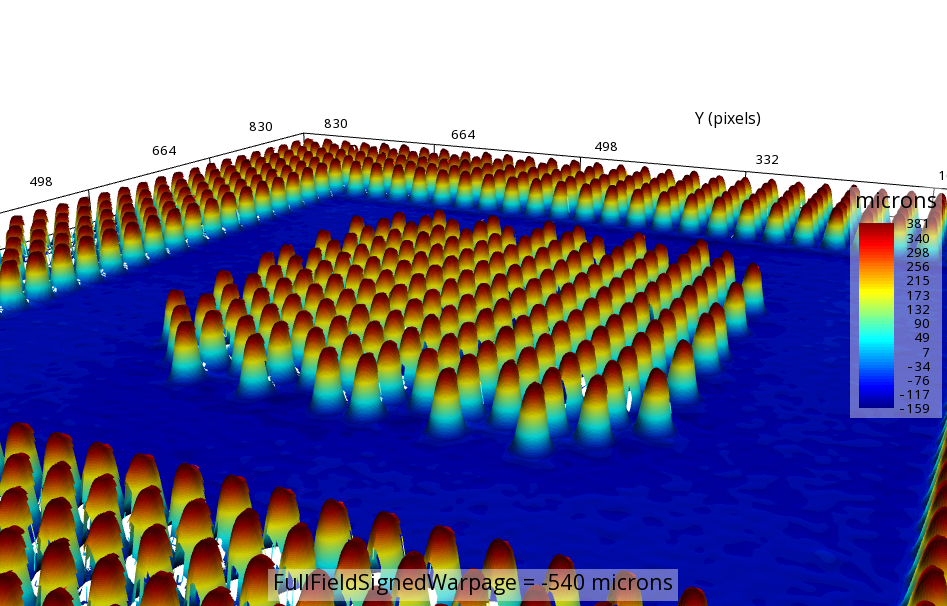
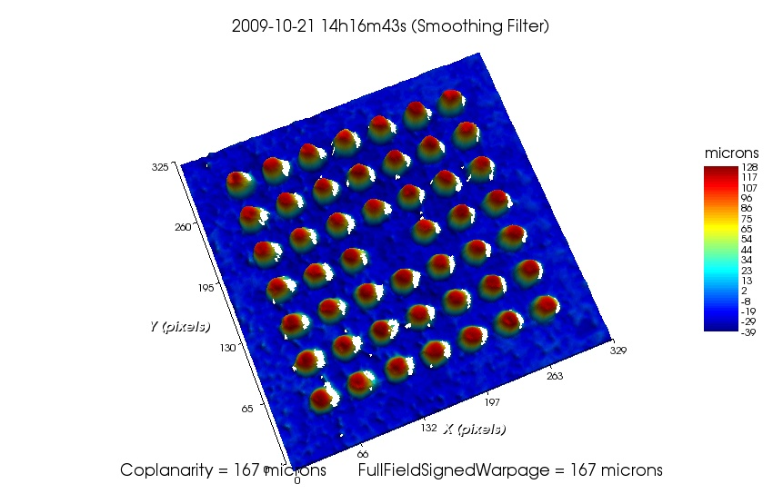
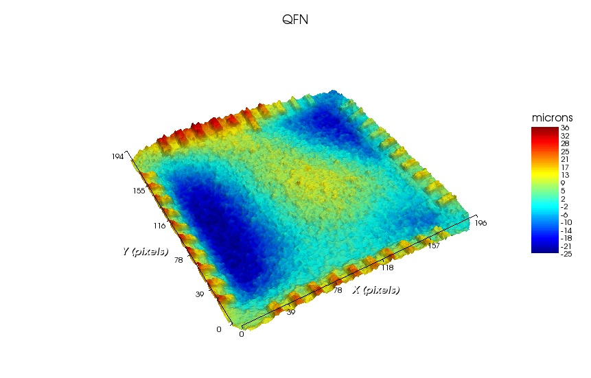
The 3D surface plots below show 2 BGA samples, a 6x6mm QFN sample, and a bare die surface.

Package on Package (PoP)
Package on Package (PoP) components, along with other 3D packaging and TSV (Through Silicon Via) technologies are becoming increasingly common, particularly in mobile devices. The trend for these package types continues toward thinner packages with higher ball pitch. As these trends increase the need for accurate warpage characterization is becoming ever more critical.
Akrometrix systems are capable of testing a range of PoP surfaces. In particular, the Shadow Moiré technique is well designed to test these sample types in high volumes through thermal cycling. Testing throughput and repeatability is increased with the addition of the Part Tracking feature in Surface Measurement, which allows automatic location, rotation, and cropping of large sample quantities in a single reflow profile.
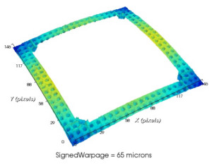
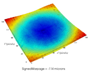
The below 3D surface plots show the shape of bottom and top components at the same elevated temperature. The top side of the bottom component is measured and, in this case, only the attaching perimeter of the sample is analyzed. The second picture shows the bottom side of the top (memory) component. Here we see that the direction and magnitude of warpage is similar for the connection between these components. This will not always be the case. Direction of warpage is important to consider when analyzing PoP attachment.
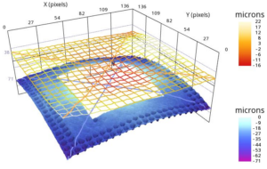
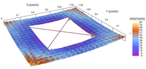
The Akrometrix Interface Analysis software allows the automatic orientation and analysis of attaching surfaces as would be the case the following example. 3D packaging presents a unique opportunity for use of the Interface Analysis software. The bottom PoP component will actually contain two attach surfaces in one component. The bottom surface will attach to a PCB and the top surface will attach to the top memory component. Below are plots from Interface Analysis showing the top (shown in wire frame) and bottom surfaces for a different PoP sample, as well as a “Gap” surface showing the difference between the two surfaces. In this case the direction of warpage is opposite for the two packages resulting in larger gaps at the package corners.
High Volume Testing
In the many years of working with leaders of the microelectronics industry, Akrometrix has seen a dramatic shift in the use of our warpage data. Originally, Akrometrix tools were most commonly used in an R&D lab for development of new technology or design comparison. With industry wide acceptance of the value of controlling and monitoring warpage characteristics for reliable SMT attachment, Akrometrix equipment is now frequently used for quality assurance. High volume thermal warpage characterization is now a common approach for lot to lot QA at the component level.
Akrometrix has accommodated this shift through a number of software developments. Our Studio software has been optimized to handle large quantities of data in a batch processing fashion. Perhaps the biggest revelation in increasing both system throughput and reproducibility between locations and users was the addition of Part Tracking. Part Tracking is a software development from Akrometrix based on edge recognition technology. This software development allows automatic locating, orienting, and cropping of low to high quantities of samples inside Studio software enabled equipment. Additionally, with the built-in Akrometrix Automated Report Generator, high volume sample results can be easily organized, quantified, and reported.
The below images highlight Akrometrix Part Tracking technology. With this approach, our customers can test large quantities of samples per thermal run in an efficient and highly repeatable fashion.
PCB Fabrication
Key industry drivers including fine pitch interconnect devices and lead-free solder temperatures are putting increased importance on substrate flatness compliance. Emerging specifications for local area (as in IPC 9641) flatness at both room and elevated temperatures are today being implemented by leading OEMs to ensure higher first pass assembly yields and field reliability.
Prototype Qualification (TherMoiré) – By measuring thermo-mechanical performance at the prototype stage, problems with new board designs can be identified, verified and documented before going into production, ensuring customer specifications are being met. Accelerating the ramp to production can reduce NPI (new product introduction) costs and reduce time-to-market for new products.
Assembly Yield and Reliability Investigation (TherMoiré) – Yield and reliability problems with a product already in production translate to increased costs as a result of waste, rework, and warranty expenses. An efficient tool for studying thermo-mechanical warpage can assist in root cause analysis and identifying the responsible party in a complex multi-organization supply chain.
Sampling Thermal Warpage for Production QC (TherMoiré) – Even after the thermo-mechanical performance of the product design is qualified, good quality products require ongoing monitoring. Unexpected changes in materials and processes are more often the rule than the exception. Testing equipment capable of handling large numbers of samples quickly in a repeatable, automated fashion can reduce inspection time and cost.
Mechanical Model Validation (TherMoiré) – Computer simulation of thermo-mechanical performance can be a powerful tool for warpage prediction, but it requires experimental verification. A measurement tool that provides feedback optimized for rapid comparison with simulation results speeds model development, confirmation of materials properties, and overall confidence in simulation results.
Outgoing/Incoming Inspection of Bare PCBs (TTSM/DFP2-LS) – Inspecting finished boards can screen for both global (overall bow and twist requirements) and local (individual component site coplanarity) warpage. The TTSM offers high throughput capabilities for measuring global and local warpage of continuous areas for PCBs up to 330x330mm. The Akrometrix DFP2-LS is available for sample warpage on samples up to 600x600mm.
Mass Lamination Process Development (TherMoiré) – Flatness inspection after lamination can identify pattern transfer problems, speeding process development by investigating temperature, pressure and stack thickness effects.
Sockets/Connectors
The Digital Fringe Projection technique is most commonly used for testing of socket and connector surfaces, due to their discontinuous nature. Along with component shapes and board local area shapes, socket warpage is also a critical component in effective SMT assembly. The Shadow Moiré technique can also be used for many socket surfaces with the appropriate data processing in Surface Analysis. The images shown to the below right are socket examples taken with the Shadow Moiré technique at room temperature and maximum temperature. Using the DFP technique attaching surfaces such as socket pin heads and connectors leads can be measured.
Shape matching of sockets and connectors can also be applied through Akrometrix’ Interface Analysis software. Sample shape can be oriented and compared with PCB local attach areas.
PCB Global and Landing Areas
PCB shape was traditionally measured at room temperature using shim gauges and a granite flat table. Shadow Moiré measurements are a far superior approach to PCB flatness characterization. Large area PCB shape can be captured at high speed and temperature without sacrificing measurement resolution. Bow and Twist standards can be applied automatically through the Akrometrix software to these global PCB measurements.
With tighter component pitches and tolerances, the warpage of PCB landing areas over temperature is becoming increasingly more critical to quantify. Akrometrix equipment is capable of capturing both global and landing area warpage at high resolution in a single thermal run. Many PCBs are known to exhibit different warpage behavior after exposure to multiple reflows. This makes capturing both global and local landing areas in a single thermal run essential. Akrometrix Surface Analysis software can batch process multiple PCB landing areas in a repeatable fashion. Additionally the fast (sub 2 second) acquisition time of Akrometrix systems is beneficial for measurement of thinner PCBs that can change shape quickly.
A PCB global and local 3D surface plot are shown below. The image on the top right is a 4x4mm PCB landing area measured with Fringe Projection.
PCB landing area data can be imported into the Akrometrix Interface Analysis software for comparison with corresponding component warpage over temperature. Having both component and PCB landing area warpage over the same temperature points and temperature profile gives customers the ability to analyze the gaps between PCB and component attach surfaces. Below, on the bottom left, a plot of a component bottom and PCB landing area is shown plotted in the Interface Analysis software. A Gap plot between these two surfaces can also be visualized as shown on the bottom right.
